- Subscribe to RSS Feed
- Mark Topic as New
- Mark Topic as Read
- Float this Topic for Current User
- Bookmark
- Subscribe
- Mute
- Printer Friendly Page
NI PCIe-1473R U16x8 DMA FIFO for Camera Link
04-26-2022 10:58 AM
- Mark as New
- Bookmark
- Subscribe
- Mute
- Subscribe to RSS Feed
- Permalink
- Report to a Moderator
I've reached out to NI engineers with this question, but wanted to ask the community for support as well. I've attached a LabVIEW project, several screenshots, and a simple NI MAX report in a .zip file.
I am trying to acquire images using a Basler acA2040-180kmNIR camera and a NI PCIe-1473R-LX110 frame grabber. The camera only supports 2- and 4-tap geometries for its 12-bit pixel mode (see image 01 in Screenshots).
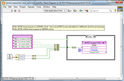
The good news: Starting from LabVIEW shipping examples for the PCIe-1473R, I've successfully implemented a 2-tap 8-bit acquisition (see images 02a and 02b in screenshots).
The bad news: I'd next like to move to a 2-tap 12-bit acquisition; however, I am unable to configure the DMA FIFO to accommodate the required data. Per the polymorphic VI selectors shown in image 03a, this requires a U16x8 DMA FIFO, but when configuring it in the LabVIEW Project, I am only able to configure up to a U16x4 DMA FIFO (image 03b).
How would I modify the FPGA code to accommodate the required data transfer? It seems like a U16x8 DMA FIFO is not supported on the PCIe-1473R and is therefore a no-go. I have peeked at the LabVIEW shipping example that demonstrates image transfer using a DRAM FIFO, and although I haven't fully understood it yet, I'm now wondering if that's the direction I have to go. Anyone out there deal with something similar or have advice?
04-26-2022 04:57 PM - edited 04-26-2022 05:01 PM
- Mark as New
- Bookmark
- Subscribe
- Mute
- Subscribe to RSS Feed
- Permalink
- Report to a Moderator
1. Does the PC and related hardware support the throughput needed?
2. You could make more than one DMA-FIFO and split the data.
I typically do not create DMA-FIFOs with the dialog box you are showing. I would use the dialog box from the target in the project. Right-click and Create new FIFO, select DMA-FIFO. See https://zone.ni.com/reference/en-XX/help/371599P-01/lvfpgahelp/fpga_creating_fifos/ (see Creating a Target-Scoped FIFO from the Project Explorer Window).
Which version of LabVIEW are you using?
Certified LabVIEW Architect, Certified Professional Instructor
ALE Consultants
Introduction to LabVIEW FPGA for RF, Radar, and Electronic Warfare Applications
04-26-2022 05:38 PM
- Mark as New
- Bookmark
- Subscribe
- Mute
- Subscribe to RSS Feed
- Permalink
- Report to a Moderator
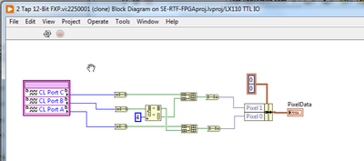
I am using 2 Tap 12 bit in my code. But my code is old. So it is not using the NI functions like the example. I am acquiring the data as fix point number.
You can create a custom data type for the FIFO and send the data as a fix point.
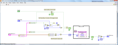
See attach diagram.
You will notice I am using frame skip when sending the images to PC.
I am working in 1250 FPS. PC can't keep up with this rate.
04-26-2022 05:39 PM
- Mark as New
- Bookmark
- Subscribe
- Mute
- Subscribe to RSS Feed
- Permalink
- Report to a Moderator
@Terry_ALE: Thanks for your response!
For #1: The camera supports 2-tap 12-bit output, and the PCIe-1473R supports Base, Medium, and Full configurations (since 2-tap 12-bit uses 24 bits of data transfer, the Base configuration should be appropriate). As far as the PC goes, the PCIe-1473R is plugged into a x4 PCIe slot (or larger slot that supports a x4 data rate), as recommended by the user guide. Is there anything else you would check in this regard?
For #2: I banged around once adding more DMA FIFOs but am really in over my head. On first pass, I added a For Loop in the 100 MHz Single-Cycle Timed Loop thinking I could do eight U16x1 writes in a row, but the FPGA compiler understandably complained that wouldn't work. My experience with the LabVIEW FPGA tools is limited to the couple days of troubleshooting I've done on this problem (I failed to comprehend when buying the card that it could only be programmed with FPGA tools). Do you have any specific suggestions of how you'd split the data among multiple FIFOs and then later recombine it? For now, I just need to acquire and transfer one camera frame (2048 pixels x 2048 pixels @ 12 bits/pixel) while avoiding overflow. Time is not a constraint.
For your last point, I have the same limitation when configuring the DMA FIFO from the Project Explorer Window and the block diagram (right-click >> Configure FIFO Type...). My options for Number of Elements per Write are 1, 2, and 4 in both cases (whereas what I seem to need is 8).
04-26-2022 05:42 PM
- Mark as New
- Bookmark
- Subscribe
- Mute
- Subscribe to RSS Feed
- Permalink
- Report to a Moderator
I forgot to add that I have VI that translate to pixel bus. I can share it.
I am not fully aware what are you trying to do. Is it just to transfer the images to the PC?
04-26-2022 05:50 PM
- Mark as New
- Bookmark
- Subscribe
- Mute
- Subscribe to RSS Feed
- Permalink
- Report to a Moderator
@AmitShachaf: Thanks for your response!
For now, I am just trying to transfer the image from the FPGA to the PC. No FPGA processing, no severe timing or frame rate constraints.
I would be very interested in looking at and trying your VIs if you can share.
04-26-2022 05:50 PM
- Mark as New
- Bookmark
- Subscribe
- Mute
- Subscribe to RSS Feed
- Permalink
- Report to a Moderator
I can help you create a simple code that will transfer the image to the PC. But in the large picture. 1473R is obsolete card. You should be using the 1477 if you are doing new design.
1473R can be programed only on Windows 7. While 1477 can be programed on Windows 10.


