- Subscribe to RSS Feed
- Mark Topic as New
- Mark Topic as Read
- Float this Topic for Current User
- Bookmark
- Subscribe
- Mute
- Printer Friendly Page
multiple ADC reads with digital output switching (external MUX)
08-28-2014 07:18 AM
- Mark as New
- Bookmark
- Subscribe
- Mute
- Subscribe to RSS Feed
- Permalink
- Report to a Moderator
First, I am using a NI USB-6363
So on an external trigger, the system I am looking to test samples 4 voltages that come out through a MUX. I have access only to the output of the MUX and want to quickly measure the voltage on all four channels. Effectively I want to have an external digital input cause:
1. Latch outputs (low going signal)
2. Sample first channel after settling
3. Go to next channel changing state of two DO lines
4. Sample after settling
5. Repeat for all 4 channels
My questions are:
1. I cannot find much about hold time with the ADC. How long must the signal be steady there? Can you start a convert, and switch the MUX before the conversion is finished without any problems?
2. When I look at my signals, they end up looking like a 4 bit counter output for counting from 0000 to 0111. From what I can gather, I cannot just get the counter bits out, but could I use multiple counters to approximate this (or is there a better way).
Overall, I am not really sure what is done on the USB-6363 and what is done on the PC. When I code with LabVIEW, it is pretty hard for me to get a good feel for what is PC and what is only done on the card and how all the timing is done. I look at a VI and I do not see a tightly timed system.
Thanks for any insights.
Chris
08-28-2014 05:10 PM
- Mark as New
- Bookmark
- Subscribe
- Mute
- Subscribe to RSS Feed
- Permalink
- Report to a Moderator
Chris,
I think I understand your system: You are using the USB-6363 for digital outputs which serve as the address inputs for the external MUX and one analog input measure the output of the MUX.
It also appears that you want to start the process when an external digital signal changes state.
Things which are not clear include:
1. Does the process stop after the 4 MUX channels have been measured one time each and then wait for another trigger?
2. How much settling time is required for the MUX?
3. What is the source impedance through the MUX (so that any additional settling due to USB-6363 input circuits can be estimated)?
4. How much difference occurs betwen the signals on adjacent channels of the MUX?
The X series manual does not mention any internal sample/hold circuitry. The analog input circuitry block diagram shown on page 4-1 and the simplified internal MUX circuitry shown on page 4-15 do not show any circuits for a sample/hold function.
My recommendation would be to assume that your MUX should remain unchanged throughout the settling time plus the sample period. So long as you are not trying to change gain ranges on the USB-6363 for different external MUX addresses, your time would be limited by the 2 MHz single channel sampling rate and the settling time, which depends on the source impedance and the size of the signal steps. The specification document has tabels and charts for estimating the settling time.
Lynn
09-02-2014 08:05 AM
- Mark as New
- Bookmark
- Subscribe
- Mute
- Subscribe to RSS Feed
- Permalink
- Report to a Moderator
Lynn, thank you for the quick reply (looks like 2 more any you hit 10k!).
1. Does the process stop after the 4 MUX channels have been measured one time each and then wait for another trigger?
Yes, stops after the four channels are read, then the whole thing is set up for another cycle (relatively slow but asynchronous).
2. How much settling time is required for the MUX?
250nS. So with 1 uS per channel, was viewing that I should have good margin.
3. What is the source impedance through the MUX (so that any additional settling due to USB-6363 input circuits can be estimated)?
Low. It is buffered by an op-amp on its end.
4. How much difference occurs betwen the signals on adjacent channels of the MUX?
All have the same range of about 2V to 0V. No range changes needed as the resolution is fine with the -10V to 10V range.
I am finding this device very much the onion problem but in reverse, every time I peel away a layer, my understanding grows on the device and then the next detail that I don't understand comes into focus.
Thanks again,
Chris
09-04-2014 01:29 PM
- Mark as New
- Bookmark
- Subscribe
- Mute
- Subscribe to RSS Feed
- Permalink
- Report to a Moderator
Chris,
Sorry for the delay in responding. Some personal issues have been occupying much of my time.
Thank you for answering the questions. One comment on the answers and then I will make a suggestion about how I might approach the issue.
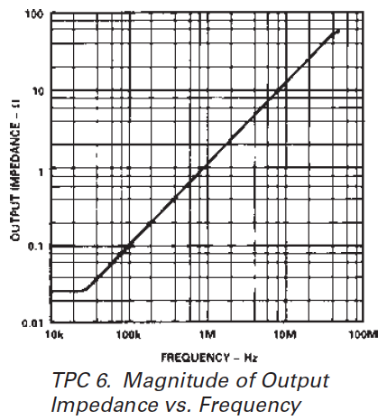
3. You are looking at a signal at the output of the MUX with a bandwidth of several megahertz. Most opamps have an output impedance which starts climbing at frequencies above a few hundred Hz to a few kHz. So the source impedance to the DAQ device may not be as low as you think. The output impedance versus frequency for the AD845 amplifier is shown below. The impedance is still low enough that it is probably not a problem with this device but your circuit may not be the same.
My suggestion: The AI and DO clocks need to be synchronized so you can keep track of the source channel for any particular sample. Although I have never done anything quite like this it appears from the specifications that you should be able to do it with the USB-6363. Configure both the AI and DO to use the same sample clock. Also configure both for finite samples and digital triggering.
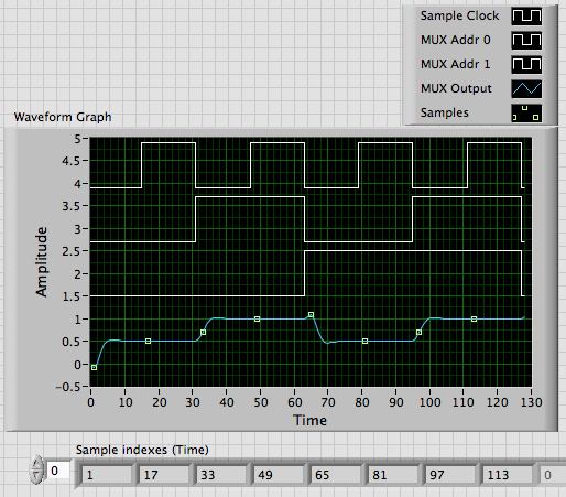
Then set the digital data to count at half the sample frequency. So the least significant bit of the MUX address will be 0, 0, 1, 1, 0, 0, 1, 1, 0 and the most significant bit will be 0, 0, 0, 0, 1, 1, 1, 1, 0. The first analog sample at each address value will be during the settling time and should be discarded. The second sample should be OK. Note that I include zeros at the end of the address set so that the MUX gets reset to zero at the end of a cycle. In the image below a sample is acquired on each edge of the sample clock. The samples at 17, 49, 81, and 113 are the valid measurements.
Lynn
09-05-2014 07:24 AM
- Mark as New
- Bookmark
- Subscribe
- Mute
- Subscribe to RSS Feed
- Permalink
- Report to a Moderator
Thanks! That looks to be good for the most part. The one question I have is that the pulse that I want to use to gate the timing is an active low signal to the DUT. But I cannot figure out how to convert a counter pulse to be low for the pulse and high otherwise. Even if I have to make a channel that is just an inverted version of the counter output, that would be good enough. I have searched around and found nothing on this.
Also, the MUX/Buffer on chip is made for driving a load quickly. The chip burns quite a bit of current to get this speed, so Zout is not going to be a limiting factor.
Thanks,
Chris
09-05-2014 04:17 PM
- Mark as New
- Bookmark
- Subscribe
- Mute
- Subscribe to RSS Feed
- Permalink
- Report to a Moderator
Chris,
I was not thinking counter, except possibly for the sample clock. The the Device will send the sample clock out on one of the PFI lines, you may not need the counter. I was thinking that the signals I called MUX Addr 0 and 1 would be hardware timed digital outputs. You would feed an array of the values listed in my previous post to the Digital Write VI.
To get the inversion you want just interchange the 1s and 0s.
Lynn
12-15-2014 06:16 AM
- Mark as New
- Bookmark
- Subscribe
- Mute
- Subscribe to RSS Feed
- Permalink
- Report to a Moderator
Okay Lynn, been a while but I needed the PCB to be built and all the other ducks in a row before "live testing" the solution you gave.
Short story: It kind of works.
Long story: I start the whole timing based on a threshold detect (negative) signal. This I use to start the timing by starting a blanking counter to keep things from getting reset by the threshold detect signal chattering. This blanking signal going low starts the MUX signals and a sample timer for the ADC. The problem is that the sample timer (using a counter) has a delay set to ~400nS (I have tried several values). 1/2 the time the delay is there sometimes it is not. Included is a scope probing of the signals for a good result, with Ch2 and 3 being the MUX0 and MUX1 lines, yellow being the sample clock (rising edge), and the green is in sync to the blanking signal but much shorter (the blanking goes for 100s of microseconds). Sometimes the yellow sample waveform is butted up to the falling edge of the green signal and sometimes as seen.
As to the LabVIEW diagram, Counter 1 is the blanking counter. It is started by an external threshold detect on PFI1. The falling edge of this counter is used for the timing of the MUX lines via counter 0 and the sample clock on counter 2. The MUX timings are perfectly syncing to the blanking signal whereas counter 2 is off sometimes.
Is this a result of counter 0/1 being more tightly coupled, or am I doing something else wrong.
Oh, the block for ctr2 being T or F, True was something else I was trying when this was not working reliably, and that doesn't work.


