- Subscribe to RSS Feed
- Mark Topic as New
- Mark Topic as Read
- Float this Topic for Current User
- Bookmark
- Subscribe
- Mute
- Printer Friendly Page
NI FlexRIO Adapter MDK Overview
11-09-2008 05:47 PM
- Mark as New
- Bookmark
- Subscribe
- Mute
- Subscribe to RSS Feed
- Permalink
- Report to a Moderator
Introduction
The NI FlexRIO Adapter Module Developer’s Kit (MDK) gives users all the tools necessary to develop a custom adapter module for use with NI FlexRIO products (like the NI 795x, 796x, 797x). This document details the contents of the NI FlexRIO Adapter MDK as well as presents a high-level technical overview of the adapter module development process.
MDK Contents
The NI FlexRIO Adapter MDK contains all information necessary to enable the user to develop a custom adapter module. It comes with extensive documentation detailing the hardware and software interfaces to NI FlexRIO. The kit includes files and examples to get started. You will receive FAM enclosures, PCB layout files, and mechanical drawings. Finally, the MDK users will have access to specialized NI FlexRIO MDK Support resources and direct technical assistance from NI R&D. The list below details the exact contents of the MDK:
Documentation
- MDK User Manual
- MDK End-User License Agreement
- MDK Info Sheet
Software
- Example Adapter Module Support files
- I2C Access Example VI’s
Hardware
- 3 blank adapter module enclosures
- 1 Windowed adapter module enclosure for probing circuitry
Design Files
- PCB Outline mechanical drawing
- Card edge connector mechanical drawing
- Adapter Module front panel mechanical drawing
Support Resource Access
- Direct R&D support via private email address
- One Hour of NI R&D schematic/layout review time
- Access to MDK community forum
Using the MDK to Create a Custom Adapter Module
The high-level steps to creating a custom adapter module are as follows:
1. Design & Build Adapter Module – Schematic, Layout, Assembly, etc.
The MDK includes all the necessary drawings, layout files, and instructions to create a PCB that will mechanically and electrically interface with the NI FlexRIO FPGA module. Files are available in standard .dxf and .dwg format for use with your own PCB design tools.
2. Register Adapter Module ID & program ID EEPROM
Instructions to program the EEPROM are contained in the FlexRIO Users Manual.
3. Create FlexRIO Adapter Module definition file (.fam)
The definition file make the module appear in the LabVIEW development environment. There are instructions and example files included in the MDK
4. Create Adapter Module CLIP (HDL & XML)
The Component-level IP (CLIP) and an XML description of the IO module establishes the mapping from your hardware to LabVIEW of individual input and output ports. The MDK contains documentation and examples of these files.
5. Write LV FPGA VI for Adapter Module & CLIP
Once all of the interfaces are defined, use LabVIEW FPGA to communicate to your custom module and develop the rest of your system. This include and FPGA design, communication across the PXI bus and a host program. The MDK includes examples and documentation.
Successful Adapter Module development requires you and/or your team have the following skills:
- PCB design – schematic & layout
- PCB manufacturing/assembly
- HDL development/integration
- LabVIEW & LabVIEW FPGA development
Adapter Module Electrical Interface
The Adapter Module interface is designed to expose the full power and flexibility of the Virtex 5 and Kintex 7 FPGA IO while keeping a general interface for diverse IO Module applications. This interface includes fixed and configurable power rails as well as defined control signals for IO Module detection and identification. Here is a summary of the physical interface between the FlexRIO FPGA and Adapter module.
Power rails
- +3.3V, +12V rails
- Configurable Vcco rail for FPGA IO banks and IO Module (set to 1.2, 1.5, 1.8, 2.5, 3.3)
General Purpose FPGA IO
- 132 Single-ended lines (configurable as 66 differential pairs) from the Virtex 5 and Kintex 7 FPGA directly connected to the IO Module
- Virtex 5 - 4 FPGA IO banks (powered by Vcco A and B)
- Kintex 7 - 3 FPGA IO banks (powered by a single Vcco)
- Trace impedance: 50 Ohm single-ended, 100 Ohm differential
Clocking
See KB for additional info on clock assignments
- Kintex 7 - Five global clock inputs from IO Module to FlexRIO FPGA
- Differential or Single Ended
- Virtex 5 - Two global clock inputs from IO Module to FlexRIO FPGA
- One 3.3V LVTTL input
- One 2.5 LVDS differential pair input
Control
- Two IO Module status handshaking signals to FlexRIO FPGA (present & power good)
- I2C bus for IO Module Identification EEPROM
Adapter Module Mechanical Details
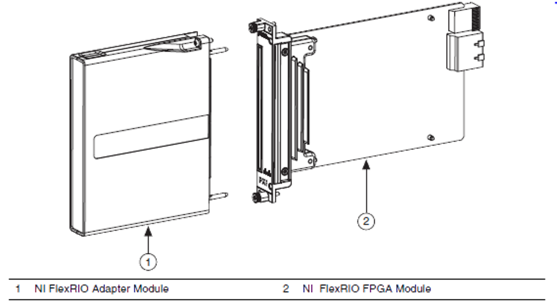
The standard FlexRIO Adapter Module design is a PCB which fits in a metal enclosure that can be mounted to the face of the FlexRIO FPGA card. It is recommended that all adapter modules conform to these mechanical requirements, although some applications may require other dimensions. Operating outside of these recommendations would require modified enclosure/mounting solutions.
Adapter Module PCB Dimensions
The Adapter Module PCB is about 3.6” wide by 4.3” tall (without including the edge connector area). This provides about 15.5 square inches for adapter module circuitry on each side. The recommended PCB thickness is .062” and the bottom side of the PCB should only be used for small passive components. The interface to the FlexRIO FPGA Module utilizes an edge connector. This removes the need for special connectors on all Adapter Modules, however does require specific PCB manufacturing specifications. Layout files and mechanical drawings of the card edge connector are including in the MDK.
Adapter Module Enclosure
The Adapter Module enclosure is a two piece clamshell design. The PCB attaches via four mounting screws. It includes alignment pins and mounting screws for connecting to the FlexRIO FPGA module. The MDK includes three total enclosures and one windowed enclosures to allow direct probing for debugging

