- Subscribe to RSS Feed
- Mark Topic as New
- Mark Topic as Read
- Float this Topic for Current User
- Bookmark
- Subscribe
- Mute
- Printer Friendly Page
Move Any Control Algorithm or Simulation Model to Embedded FPGA Hardware with New Floating Point Toolkit
09-28-2014 03:38 PM
- Mark as New
- Bookmark
- Subscribe
- Mute
- Subscribe to RSS Feed
- Permalink
- Report to a Moderator
Move any Control Algorithm or Simulation Model to FPGA Hardware with New Graphical Floating Point Toolkit
A new Heterogeneous FPGA Graphical Floating Point Toolkit is now available. Using the toolkit, you now can move virtually any advanced control algorithm or simulation model to cost effective LabVIEW RIO embedded systems for high speed, deterministic execution in heterogeneous FPGA hardware.
The Heterogeneous FPGA Graphical Floating Point Toolkit (download) also includes example designs for state-space, transfer function, 3-phase induction motor real-time HIL simulation and 3-phase induction motor direct torque control.
Motivation
- Enable virtually any control algorithm or simulation model to be moved to high speed FPGA hardware
- Provide the ability to achieve required execution speed while minimizing resource consumption
- Bring the power of FPGA hardware acceleration to non VHDL/Verilog programmers
- Eliminate float to fixed point conversions
Benefits
- Eliminate time consuming and error prone floating to fixed point conversion
- Avoid numerical stability issues associated with fixed point control design & simulation algorithms connected in series and feedback paths
- Minimize engineering effort to move complex algorithms from desktop or real-time environments to hardware accelerated FPGA hardware
- Leverage the higher performance-per-dollar, performance-per-watt and performance-per-chip of highly parallel execution in heterogeneous FPGA hardware
Use Case Examples
- Porting advanced control algorithms from desktop simulation environments to high speed execution on deployable embedded system hardware:
- Field oriented control
- Direct torque control
- Transfer function/state space compensators and observers
- Predictive control
2. Porting simulation models to FPGA hardware for real-time simulation:
- Systems of transfer functions
- Systems of state-space models
- Power electronics circuit simulation
- Microgrid simulation
- Motor/generator simulation
- Design space exploration and global optimization
3. Hardware acceleration of digital signal processing algorithms to offload processor:
- True RMS power metering
- Active/reactive power and power factor calculations
- Total harmonic distortion
- Health monitoring and predictive maintenance
What is Heterogeneous FPGA Hardware?
Most FPGA devices today are actually a heterogeneous system on a chip (HSOC). Rather than containing programmable logic only, heterogeneous field programmable gate array (FPGA) hardware contains an array of integrated digital signal processor (DSP) cores capable of efficiently executing math operations, and in some cases also contain one or more microprocessor in the same chipset. These modern FPGAs are actually hybrid computing devices, utilizing a combination of reconfigurable logic slices and DSP cores. Hard-core DSP processing elements act as highly optimized math engines to achieve the excellent performance-per-dollar and performance-per-watt traditionally associated with monolithic digital signal processor (DSP) devices. Because these mini DSP ASIC chipsets are distributed throughout the programmable logic fabric, capable of providing custom data communication paths between the distributed DSPs, these HSOC devices are able to obtain a much higher level of parallelism than traditional Von Neumann computing architectures, which suffer from diminishing returns as more processing cores are added due to communication overhead. In HSOC devices, the reconfigurable computing fabric provides high speed programmable communication logic for data transfer among the massively parallel computing elements.

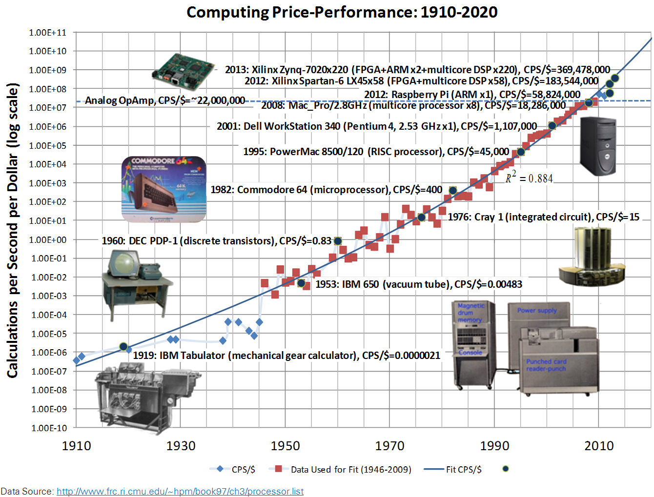
Due to this unique reconfigurable I/O (RIO) architecture, HSOC devices are capable of achieving massive parallelism with the cost advantage that comes from integrating all of the heterogeneous computing functionality on a single silicon die. In the chart below, the performance of the Spartan-6 LX45 Heterogeneous FPGA (sbRIO-9606 and General Purpose Inverter Controller) and Zynq-7020 Heterogeneous FPGA (cRIO-9068 and sbRIO System on Module) are compared to a traditional monolithic dual core DSP (C6000 series).

The chart below shows computing performance-per-dollar from 1910 to present, with a power law curve-fit equation extending into the future. Since the clock rates for individual computing elements have reached thermal limits, the trend in recent years is to utilize a large number of computing elements executing in parallel to achieve higher performance-per-dollar. At the forefront of the Moore's Law curve today are heterogeneous system on a chip (HSOC) devices that are capable of implementing algorithms in a massively parallel fashion due to their unique distributed computing hardware architecture: A mix of programmable logic, DSP cores and microprocessors and programmable communication logic which provides custom high speed, low latency data communication links between the computational elements. By contrast, traditional Von Neumann architecture computers suffer from diminishing returns as additional processing cores are added because data communication latency becomes the performance bottleneck.
List of IP Cores Included with the Toolkit
- Low Pass Filter
- Single-Phase PLL
- PI Float Simple Multichannel
- PI Float Simple Singlechannel
- PID Float Simple Multichannel
- Transfer Function Solver Multichannel (Speed Optimized)
- Transfer Function Solver Multichannel (Resource Optimized)
- State-Space Solver Multichannel (Speed Optimized)
- State-Space Solver Multichannel (Resource Optimized)
- IGBT Inverter Model
- 3-Phase Squirrel Cage Induction Motor Simulator
- Clark Transform (ABC to alpha-beta)
- Inverse Clark Transform (alpha-beta to ABC)
- Park Transform (ABC to DQ)
- Runge-Kutta 1 (RK1) Differential Equation Solver
Two Types of Graphical Floating Point Math Operators
The toolkit offers two types of FPGA graphical floating point math functions:
- 1. IP cores designed to minimize resource consumption
- 2. IP cores designed to maximize performance
These two types of IP cores are explained below.
1. IP cores designed to help you minimize resource consumption on cost optimized embedded systems like the NI Single-Board RIO General Purpose Inverter Controller (GPIC). These are the easiest to use cores, and are intended for use outside the Single Cycle Timed Loop (SCTL) structure in inside normal while loops.
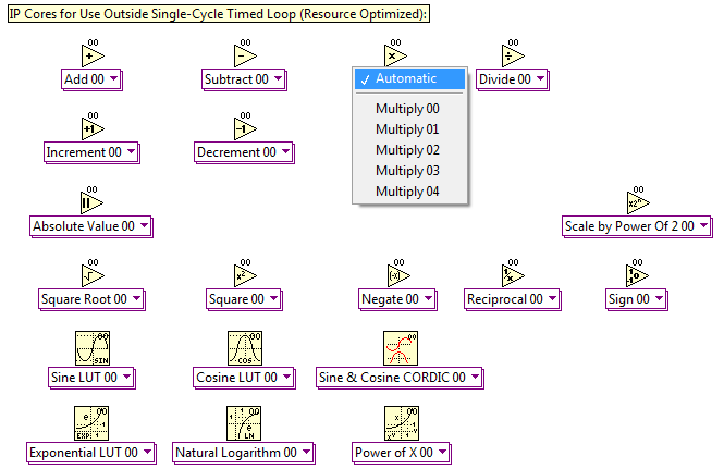
The cores are non-reentrant, enabling automatic reuse of the floating point math operations to minimize resource consumption. For example, if you drop the Multiply 00 function (see below) in your application 20 times, there is actually only a single instance of the math operation that is shared among all 20 callers. The LabVIEW FPGA compiler automatically inserts arbitration logic to multiplex the execution among all of the callers. Thus, the utilization of FPGA resources (slices, DSP core multipliers, etc.) only increases slightly as you add more Multiply 00 operations. However, the timing performance of the loops containing the Multiply 00 operator decreases as you add more operations, since it's a resource shared by all of the callers. If higher speed performance (lower latency) is required, right-click on the polymorphic subVI and select a different/independent instance, such as Multiply 01. The performance increases since there is less sharing of resources. It is important to measure the loop rate of each loop containing non-reentrant functions to determine the proper tradeoff between execution speed and resource utilization.
In this way, the FPGA Graphical Floating Point Toolkit is designed to enable you to achieve the timing performance your application requires, while simultaneously minimizing the amount of FPGA resources utilized. Furthermore, very large and complex floating point applications can be fit on relatively modest and low cost FPGA targets.
For example, in fixed point math, one developer was unable to fit an advanced field oriented control algorithms for a back-to-back power converter on the Spartan-6 LX45 FPGA of the NI sbRIO General Purpose Inverter Controller (GPIC). This included fixed point ABC to DQ transforms, with custom PLL, multiple PID controllers, notch and low-pass filters, etc. We did a find & replace in LabVIEW to convert all of the fixed point math operations (multiply, add, subtract, divide, etc.) to resource optimized (non-reentrant) cores from the new toolkit. By converting to a common floating point data type, and reusing the same floating point math operators throughout the application, the floating point version of the application compiled and ran on the modest Spartan-6 LX45 target (58 DSP cores) with all loop at rates executing at rates exceeding 100 kHz. (The minimum required loop rate for this application was 10 kHz). Below is an ABC to DQ transform operation in floating point math. Note the “00” labels indicating that only a single shared instance of each floating point operator is being used.

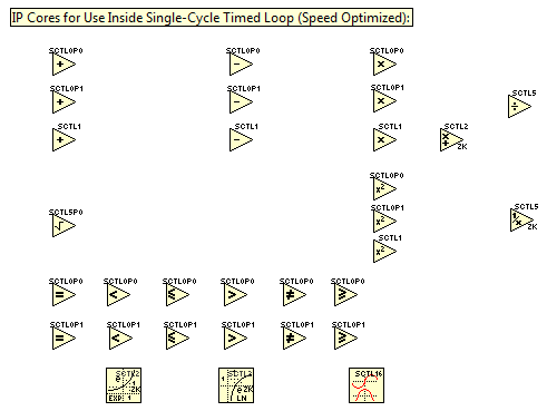
2. IP cores designed to maximize performance as necessary to obtain the speed required (typically > 500 kHz) for applications such as real-time HIL simulation of switched mode power electronics and other cyber-physical systems (CPS). These high speed IP cores are currently supported on SPARTAN6, ZYNQ, and KINTEX7 heterogeneous FPGA targets. Most operators are provided with several latency and pipelining options, designed to accommodate different programming styles.
Key Concepts
Using floating point math operators inside the Single Cycle Timed Loop (SCTL) requires an understanding of several key concepts.
A. LabVIEW FPGA Single-Cycle Timed Loop (SCTL)
By placing your graphical programming code inside a Single-Cycle Timed Loop (SCTL), you are instructing the LabVIEW compiler that all of the functionality must be executed within a single FPGA clock tick, which is typically 25 nanoseconds (40 MHz) by default. Because your logic is implemented combinatorially in hardware (with no shift registers acting to synchronously clock data between operations), the code often uses less resources than a single instance of the same logic placed outside of an SCTL. However, there can be no sharing of resources inside or between SCTLs (with the exception of certain specially designed functions such as FPGA RAM access, FPGA registers, and local variables). By placing your algorithms inside an SCTL, you are instructing the compiler to produce a highly parallelized, speed optimized implementation of your algorithm.
Note that it is possible to create a derived clock and configure it for a rate faster or slower than the base clock rate in rational multiples (i.e. 180 MHz (9/2), 20 MHz (1/2), etc.). The maximum rate at which you can execute the floating point math operations depends on the type (i.e. SPARTAN6, ZYNQ, KINTEX7) and speed class (i.e. -1, -2) of the FPGA for which you are compiling. The Heterogeneous FPGA Graphical Floating Point Toolkit functions are designed to ensure that all floating point math functions can compile within a 40 MHz clock rate on all supported targets.
Learn more about the LabVIEW FPGA SCTL.
B. Latency, Pipelining and Handshaking
Many individual floating point math operators (i.e. multiply, add, subtract) can be executed within a single 25 nanosecond clock tick. These functions are marked with the label beginning "SCTL0". However, because the floating point math takes the majority of the 25 nanosecond loop time, a pipelining stage is required immediately after the floating point operator. On the following clock cycle, the results from the previous cycle are immediately available at the output of the pipeline function (feedback node). In this way, multiple floating point operations can be executed sequentially in a SCTL while meeting the timing requirements of the loop.
The Heterogeneous FPGA Graphical Floating Point Toolkit functions labeled "SCTL0P0" do not contain an internal pipeline operator. Therefore, you must place pipeline operators between each function, as shown in the example below. This SCTL solves the mechanical equations for a 3-phase induction motor in real-time. Note that there are seven pipeline stages, so the last result (electric speed out) is available on the 8th iteration of the SCTL. Therefore, the stop condition for the loop occurs when the counter has incremented from 0 to 7. To facilitate timing analysis, the pipeline stages are arranged in vertical columns. At the beginning of iteration 1, the results of the four multiply operations on the left are available at the output of the left most pipeline operators. The subtract and add operations produce valid results by the end of iteration 1, which are available at the beginning of iteration 2. At the beginning of iteration 3, a valid calculation for motor torque is available (ElectricalTorque = (AlphaFlux*Beta_Current - BetaFlux*Alpha_Current)*MotorPoles*1.5).

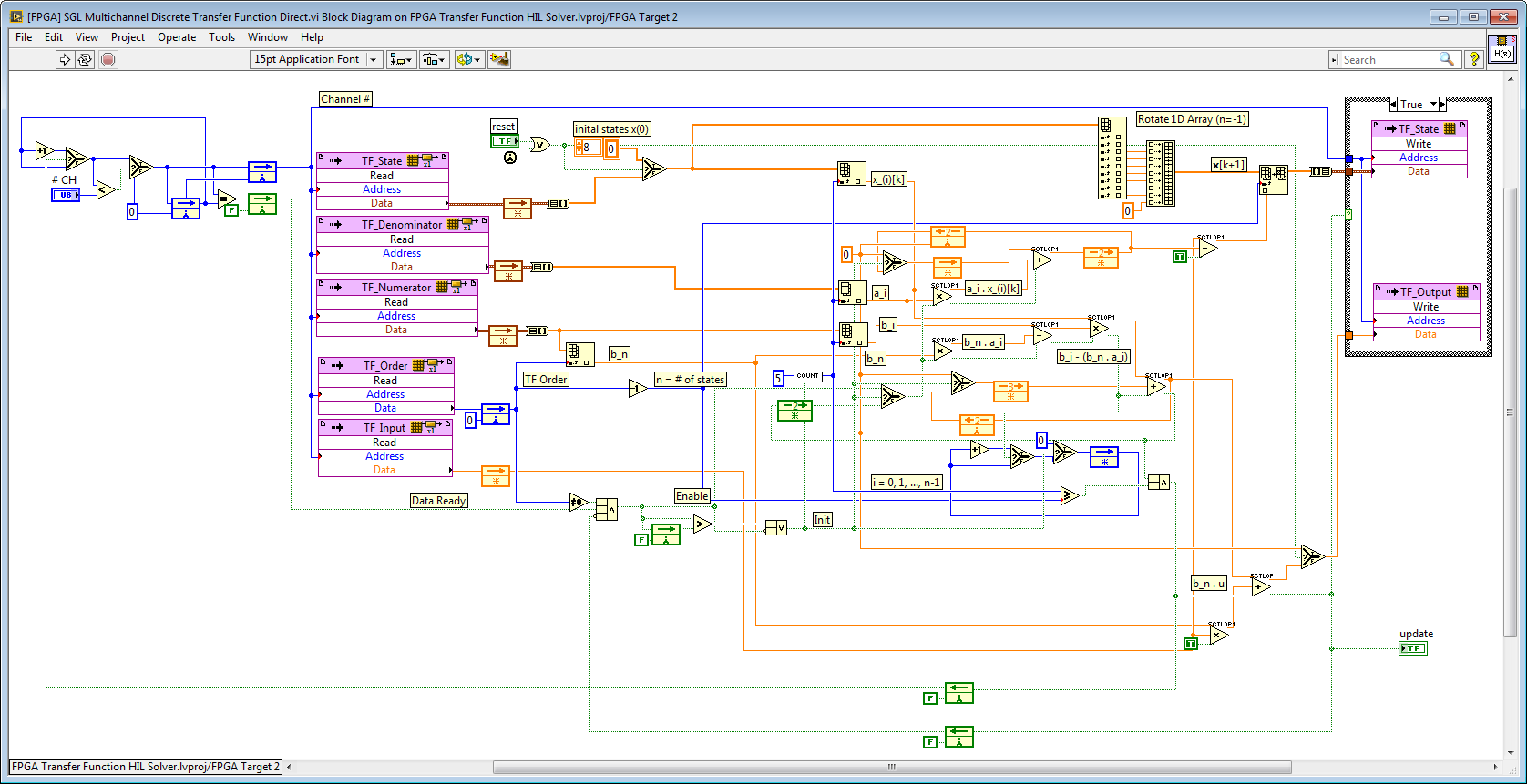
The Heterogeneous FPGA Graphical Floating Point Toolkit functions labeled "SCTL0P0" contain a built-in internal pipeline operator. Therefore, it's not necessary to place additional pipeline operators (feedback nodes) between each function, as shown in the example below. However, the execution timing can be analyzed used the approach described in the paragraph above. The algorithm below is a speed optimized discrete-time transfer function solver designed to support up to 9th order transfer functions. By utilizing FPGA RAM to store the transfer function coefficients and state, any number of independent or coupled transfer functions can be solved without increasing FPGA resource utilization. Therefore, this is called a "multichannel" transfer function solver.
The Heterogeneous FPGA Graphical Floating Point Toolkit functions labeled "SCTL1" are designed for an internal latency of 1 clock tick. Therefore, no pipeline stage is required after the floating point operators. The algorithm below is a Runge-Kutta 1 (RK1) solver for the speed optimized state-space solver. RK1 is perhaps the most common numerical method to find a numerical solution to ordinary first order differential equations (x

Some functions takes more than one clock cycle to execute, such as Multiply Add Float SCTL 40 MHz Latency 2 (Zynq and Kintex-7 Only).vi. The results appear two clock cycles after appearing at the inputs, so the label "SCTL2" is used. In other words, x
.png)
Other functions, such as division, take more cycles to execute. In the case of Divide Float SCTL 40 MHz Latency 5.vi, the inputs from one iteration appear at the output result terminal 5 cycles later. Therefore, the label "SCTL2" is used. In other words, x/y
In this case, handshaking functions are included to signify when data is available. For example, if enable is true on the first iteration and held true, then data valid will be true on the 6th iteration and subsequent iterations. Alternately, if enable is set true for only a single iteration, then data valid will be true only on the 6th subsequent iteration.

- C. Why Not Use Fixed Point Math? (Background and Motivation)
In the past, it took large amounts of engineering effort to move control algorithms and simulation models into FPGA hardware, due to the need for PhD level numerical expertise required to convert the algorithms to reliable fixed point math implementations. It has not been possible to fully automate the process of float to fixed point conversion. Furthermore, a lot of assumptions need to be made to create an efficient fixed point version of the algorithm and the resulting implementation is typically very numerically brittle. In other words, if the assumptions are changed, the float to fixed point conversion process must be started over. An example of such an assumption is the range of the physical signal inputs to an algorithm. A fixed point PLL algorithm designed for an input voltage range of +/- 10 Volts will need to be redesigned if the input signal range is changed to +/- 400 Volts.
Discrete time control design and simulation algorithms go numerically unstable in the case that two discrete poles overlap or reach the edge of the numerical stability boundary (the edge of the real-imaginery unit circle). As you can see in the example below for a second order system such as an RLC circuit or mass-spring-damper, in fixed point numerical instability typically occurs at 40 kHz and faster loop rates because fixed point rounding tends to place the poles on top of the stability boundary due to rounding. By contrast, a single precision floating point implementation could execute at rates exceeding 3 MHz without numerical stability issues.

More vexing is the issue of overlapping poles, which tends to happen in fixed point due to rounding. The issue of overlapping poles is considered a "showstopper" for many control design and simulation algorithms for the following reason: Although an individual algorithm may be designed to avoid such numerical instability, it is difficult or impossible in practice to ensure numerical stability when individual algorithms are connected in series or with feedback paths.
Take for example, the series and feedback connection of two linear transfer functions, G1(s) and G2(s). The connection drawings and equivalent transfer functions are shown below.


In the feedback connection case, the equivalent transfer function is G1(s)/[G1(s)+G2(s)]. While the fixed point implementation for each individual transfer function may be numerically stable, the feedback connection may not be stable because pole overlap may occur in the equivalent transfer function. Therefore, it is not feasible to adopt a modular programming methodology and unit test approach for fixed point control design and simulation algorithms, since such an approach cannot guarantee numerical stability when each individually validated unit is interconnected. Also, it is common to interconnect the transfer functions in a plurality of ways during the control design process, as in the case of cascaded control loops. Therefore, analyzing all of the potential numerical stability problems that might occur and designing the fixed point word lengths to ensure stability in all cases is not feasible. Even if it were feasible to anticipate all interconnection schemes and design for them, the resulting transfer functions would likely utilize very large fixed point word lengths that consume more FPGA hardware resources than a single precision floating point implementation.
Important Development Practices
- Using Find and Replace to Substitute Math Operators
Below is an example from an induction motor direct torque control example for the sbRIO GPIC, developed by Pedro Ponce Cruz of ITESM. To convert all of the math operators to floating point, click on an operand like the fixed point math Multiplier shown below, then navigate to Edit>Find and Replace (Ctrl-F). Select the equivalent floating point operand from the FPGA Graphical Floating Point Toolkit (..\IP Cores\IP Cores - LabVIEW FPGA\Floating Point\Multiply Float.vi) and Replace All.
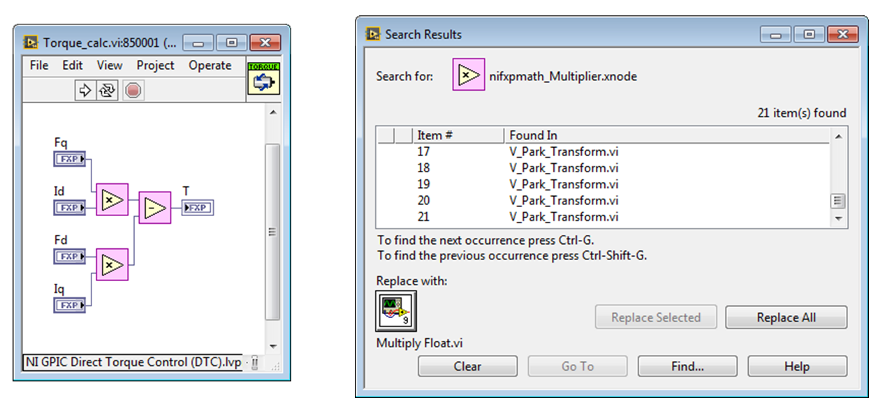
The updated, resource optimized floating point version of the torque calculation VI is shown below. Note that all three input terminals were selected at once and converted to single-precision float via the property page.

The conversion process took 15-20 minutes. The converted application is shown below.
 Application - Float.png)
The FPGA resource utilization of the original fixed version versus the resource optimized floating point version is compared in the table below. The floating point direct torque control (DTC) analog input and control loop executes at a maximum rate of 23 microseconds (43 kHz). Based on the electrical time constant of the motor, the required loop rate is 200 microseconds (5 kHz).
Original Fixed Point Version | Resource Optimized Floating Point Version |
Total Slices: 57.5% (3921 out of 6822) | Total Slices: 65.5% (4465 out of 6822) |
Slice Registers: 16.1% (8766 out of 54576) | Slice Registers: 21.7% (11821 out of 54576) |
Slice LUTs: 43.2% (11787 out of 27288) | Slice LUTs: 47.7% (13003 out of 27288) |
Block RAMs: 9.5% (11 out of 116) | Block RAMs: 10.3% (12 out of 116) |
DSP48s: 100.0% (58 out of 58) | DSP48s: 15.5% (9 out of 58) |
Efficient Analog Input Scaling
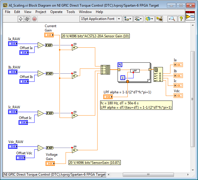
The subsystem for scaling the analog inputs from raw integer values to scaled floating point values with SI units (Volts, Amps, etc.) is shown below. By reading the analog inputs in raw integer format (see above), the FPGA resource utilization of the I/O node is minimized. Removing offsets is done using integer subtract operations, and then the conversion to scaled floating point units (including the sensor gain) is done in a single step.
Handling State and Configuration Information in Multichannel IP Cores
The multichannel floating point low pass filter IP core is also used. It provides a run-time changeable low pass filter frequency coefficient (LPF alpha). The Channel # address input is wired to the iteration terminal on the For Loop in the calling application (see above).
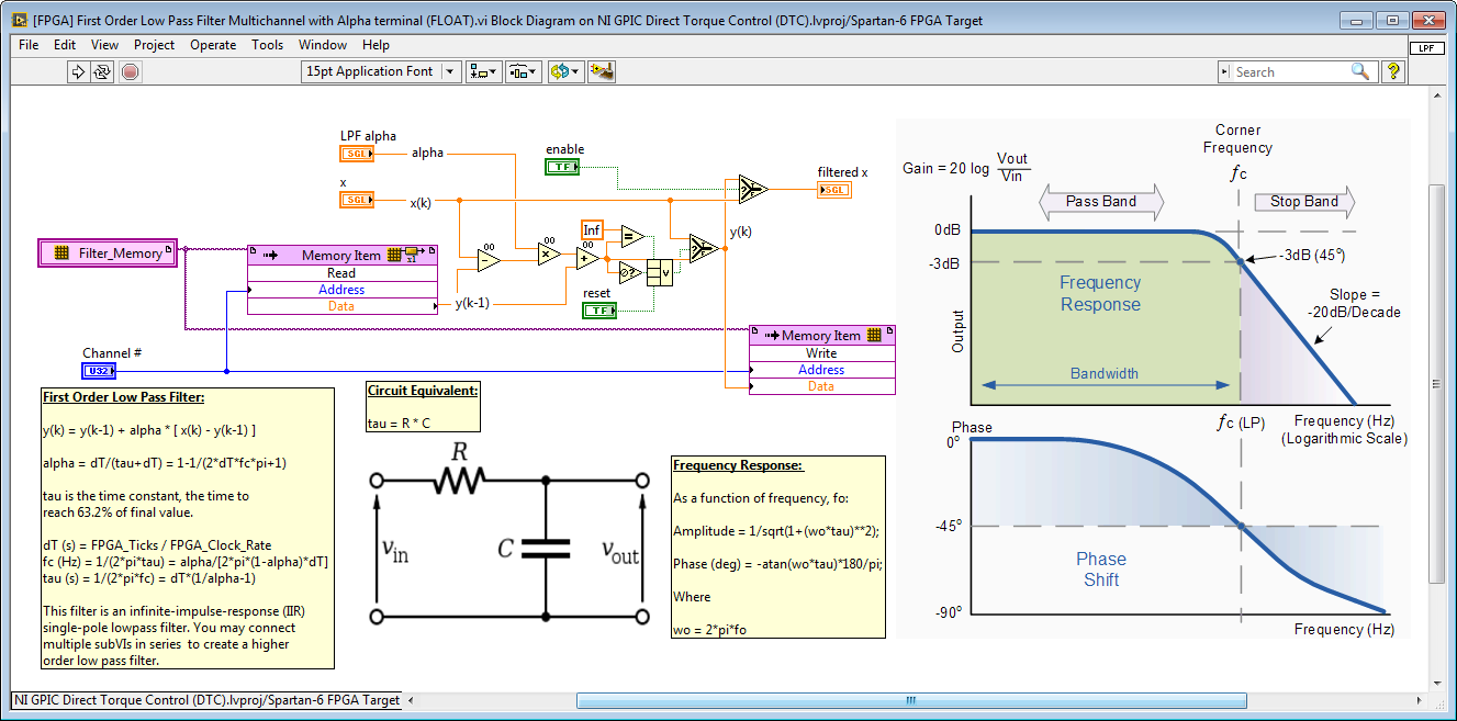
Note that the low pass filter IP core itself is configured for non-reentrant execution. By passing in a Channel # address value from the calling VIs, the core is able to hold the state values for each caller in a unique FPGA RAM memory location and thereby produce the correct result for each channel. In general, you will need to create an addressing scheme for any non-reentrant IP core that holds internal state or configuration values which are unique to each channel.
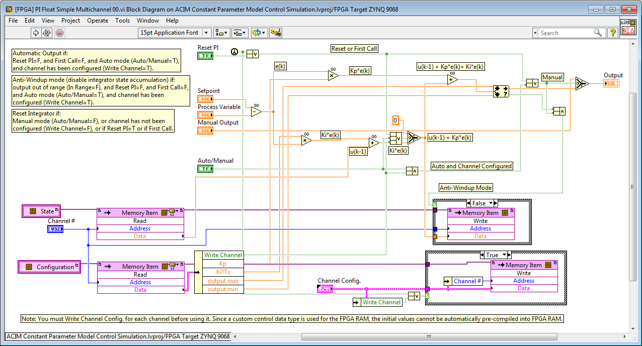
A general example of a state and configuration addressing scheme is illustrated by the “[FPGA] PI Float Simple Multichannel 00.vi” IP core shown below.
Note that a custom control data type is utilized for the Configuration data, which enables the configuration data to be written or read in a single FPGA clock tick, rather than taking one clock cycle per value. Be aware that using a cluster can result in a less efficient utilization of FPGA RAM. Top level front panel controls/indicators for clusters utilize also more slices than more simple data types. On the other hand, a benefit of using clusters is that all of the internal register values are updated synchronously, which is important for some use cases.
Also note that VI-Defined Memory configurations are used to make the IP Core more portable. Otherwise, the end user would need to create the appropriate FPGA RAM item in the LabVIEW Project tree or the IP core would show an error condition. In some cases, it may be desirable to use LabVIEW Project defined memory, such as the analog input scaling/gains and fault limit settings of the GPIC Reference Design application where it is important for the user to customize these values for their particular application requirements.
2. Minimizing Resources: Utilizing Non-Reentrancy to Share Resources
In the example below, all of the floating point operators are non-reentrant. Therefore, there is only one multiply operation and one subtract operation that is being reused multiple times. Because of the re-use, the FPGA resource utilization is much lower. However, the performance will be lower because of the time multiplexing of the shared resource. Most floating point math operations execute in 25 nanoseconds, which is typically much much faster than the required execution rate for control and signal processing algorithms. Therefore, it is often a good design decision to reuse the math operators.
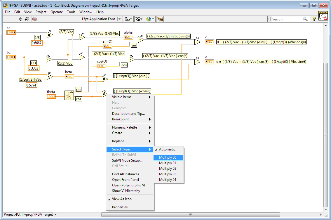
3. Understanding the Impact of Shared Resources on Execution Timing and Execution Order
When using non-reentrancy to share resources (see above), it is important to understand the implications for the execution timing and execution order of the FPGA code. The LabVIEW FPGA compiler automatically generates logic to multiplex access to the shared resources. However, because the execution order is typically not explicitly defined, the execution order may be different each time you compile the FPGA application.
However, assuming the execution speed of the shared floating point math operations is much much (>>) faster than the specified loop rate, the impact on your application performance is negligible. On the other hand, if the loop rate for the algorithm is close to the execution time of the shared floating point math operations, the impact of resource multiplexing may be significant. This is particularly important for applications containing multiple loops executing at different rates that all share the same floating point operators. In this case, the simplest solution is to use separate polymorphic instances of the floating point operators in each loop so there is no resource sharing between loops. However, the FPGA resource utilization increases significantly if separate copies are used, and assuming the floating point math operations execute much much faster than the specified loop rates, the impact of resource sharing on execution timing and execution order can be neglected.
In any case, it’s important to benchmark the performance of any loop containing shared (non-reentrant) floating point math operators to identify whether the execution speed is much much (>>) faster than the specified loop rate. If it is not, then the impact of resource multiplexing should be analyzed after each compilation. Code to measure the achieved loop rate should always be included, as shown below.
 Application - Float.png)
In this particular case, the required loop rate is 200 microseconds and the achieved loop rate is 23 microseconds. This is verified by setting DTC Rate (uSec) to 0 and observing the DTC dT (us) indicator. Therefore, execution speed (23 us) is >> than specified loop rate (200 us), so the impact of resource multiplexing on execution order and execution timing can be neglected.
4. Using LabVIEW FPGA Desktop Execution Node to Simulate and Test Before You Compile
The LabVIEW FPGA Desktop Execution Node (DEN) can increase your development productivity by orders of magnitude. Don't wait for a long FPGA compile to complete and then testing your FPGA applications running in hardware with limited debugging tool support. Instead, simply right-click to put your FPGA application in simulation mode and create a testbench application using the LabVIEW FPGA Desktop Execution Node.
As shown below, the NI LabVIEW RIO toolchain supports time-adaptive co-simulation of cyber-physical systems. The FPGA application is put into simulation mode and co-simulated with a physical modeling environment such as NI Multisim. The patented NI toolchain automatically keeps the two simulations synchronized, and automatically adjusts the simulation timestep to accurately model the closed-loop dynamic interaction between the FPGA control system and the physical world to which it is connected. By contrast, most co-simulation tools used fixed timesteps, which requires the user to know the appropriate timestep and set it before the simulation is executed. In practice, the required timestep varies based on the dynamics of the system and should be continually adjusted to ensure accurate results—particularly during transient events like short circuits, inrush or faults.
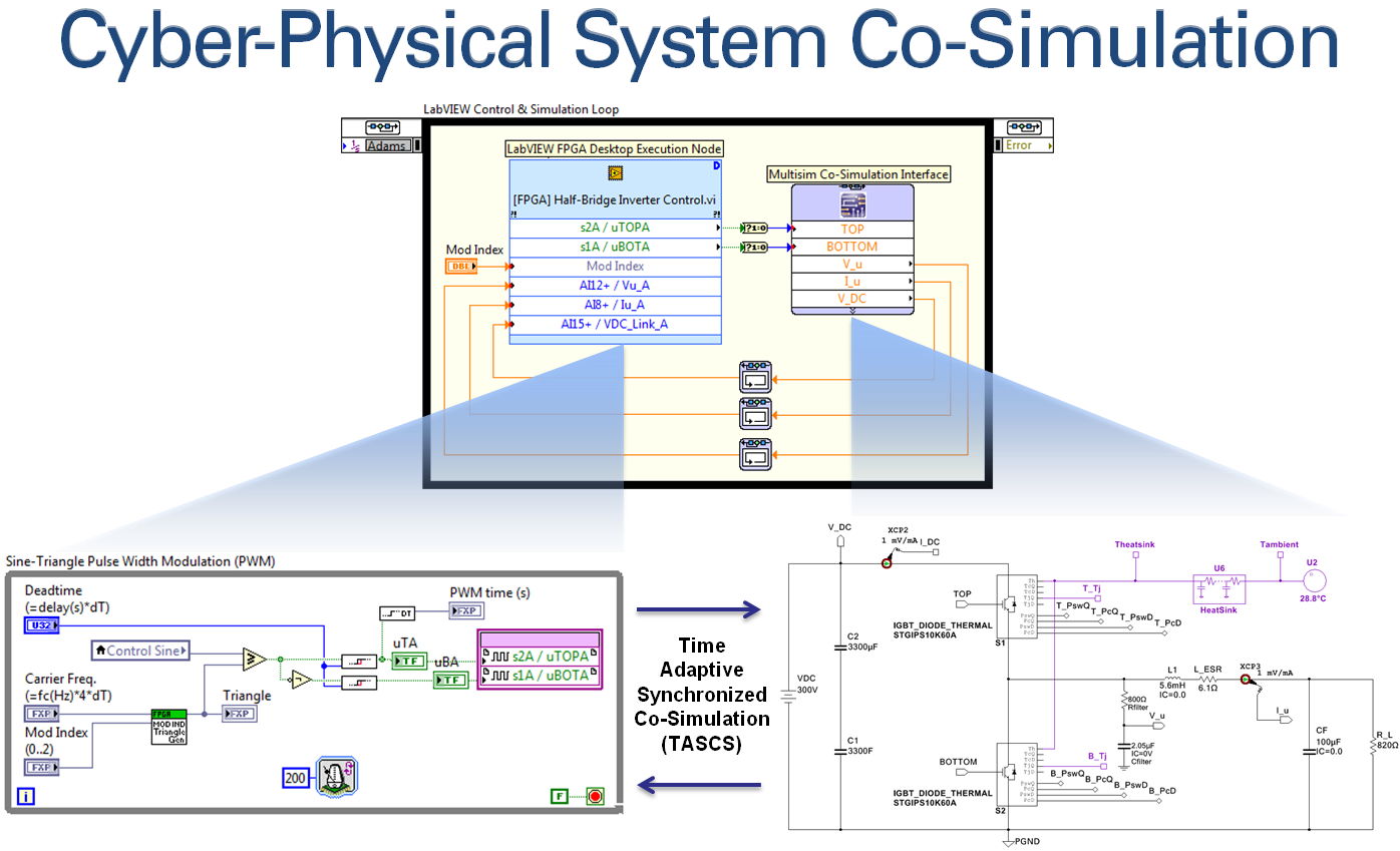
Note that the LabVIEW FPGA Desktop Execution Node also enables you to read or write all of the input-output values of the FPGA application from your testbench application—enabling you to feed in test signals such as:
- Recorded signals from acquired data
- Simulated I/O signals from software function generators (i.e. noisy sine wave)
- I/O signals from a variety of simulation environments, which are co-simulating in a time synchronized manner (i.e. 1 microsecond of time in the FPGA application is 1 microsecond of time in the simulation model)
Let’s examine a simple example of an FPGA algorithm for pulse width modulation. This example is taken from the GPIC Reference Design project. For a sensorless control application, we'd like to add some clock signals to the pulse width modulation (PWM) function below to trigger the sampling of voltage and current at certain precise instances during the PWM cycle. For this particular application, we want to calculate the rate of change of current with respect to time while applying either +VDC or -VDC to the inductive load using a full-bridge power converter. To obtain the best measurements for the sensorless inductance calculation, we decide to sample voltage at the mid-point of the PWM on and PWM off time, and the current at the beginning and end of the PWM on time. We also want to adjust for the delay between when we set the simultaneous analog to digital (ADC) sampling trigger and when the physical convert operation occurs in the ADC chipset.
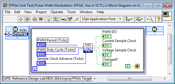
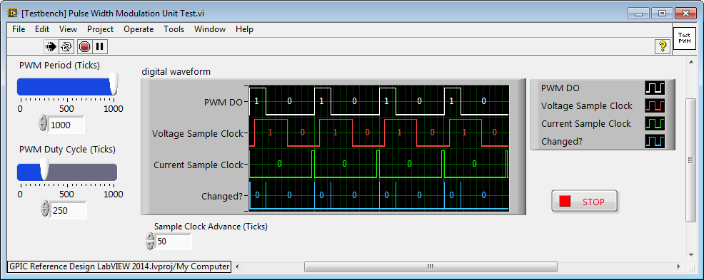
Using the LabVIEW FPGA Desktop Execution Node (DEN), a unit test application is built that enables us to exercise the PWM IP core and modify the logic to match our application requirements. The testbench enables us to access the front panel controls and indicators of the FPGA application (on every simulated 40 MHz clock tick), and plot the digital outputs of the IP core on a digital waveform graph for a logic analyzer type display.

Analysis of the "logic analyzer" testbench graph reveals that the Voltage Sample Clock is producing the desired waveform. By triggering the analog to digital converter on the rising edge and falling edge, the voltage applied at the inductive load terminals can be sampled at the mid-point of the on-time and off-time respectively. On the other hand, the Current Sample Clock is not producing the desired waveform needed to produce the desired ADC triggering signals. Instead, we would like it to go true a certain number of cycles before PWM DO goes true and go false a certain number of cycles before PWM DO goes false, where the number of cycles are determined by the Sample Clock Advance (Ticks) terminal.
While the FPGA application is being simulated, all of the debugging features of LabVIEW are available. In the example below, probes, conditional probes and highlight execution is used to understand the existing logic for the Current Sample Clock so it can be modified to match the application requirements.

4. Simulating Ideal Math Operators vs. Xilinx CoreGen Behavior
The high speed floating point math operations have internal conditional compile structures that enable you to select between simulating the ideal behavior or the simulated behavior of the internal Xilinx CoreGen logic. By default, the ideal behavior is simulated to provide faster simulations. Let's say you are adding your own extensions to the Heterogeneous FPGA Graphical Floating Point Toolkit, or you want to test the behavior of the existing items in the palette. In this case, right click on the FPGA target and navigate to properties. Then add a Conditional Disable Symbol called "SIMULATE_XILINX_IP" and set its value to "TRUE".
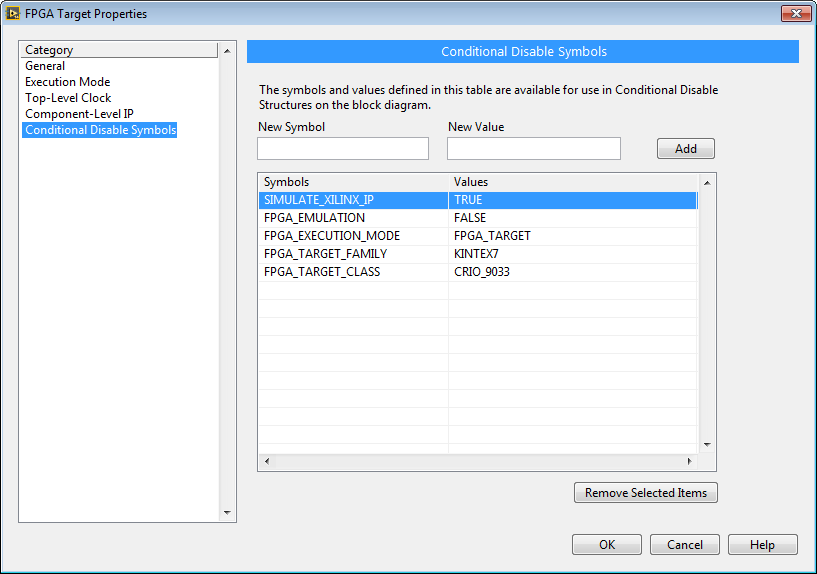
5. Using single-step deployed execution for validation and co-simulation
This technique is useful for validating FPGA based simulation models or control algorithms against a "gold standard" trusted algorithm. To do it, first create a "single step" version of the FPGA application, as shown below for the state-space solver. Rather than automatically advancing each time step, if Autostep is false then the value of the Step input must be changed in order to advance time.
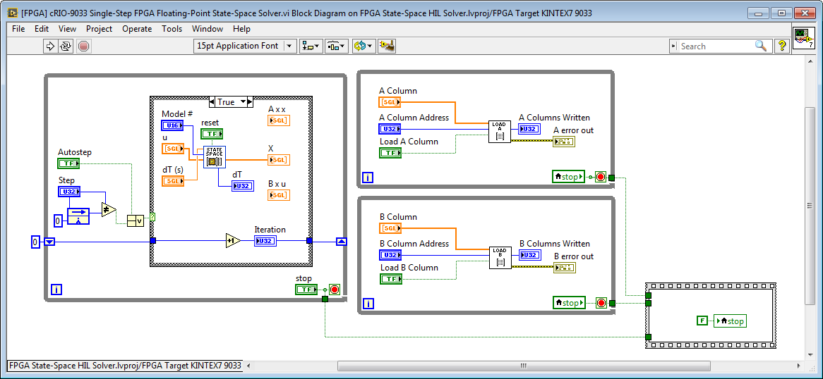
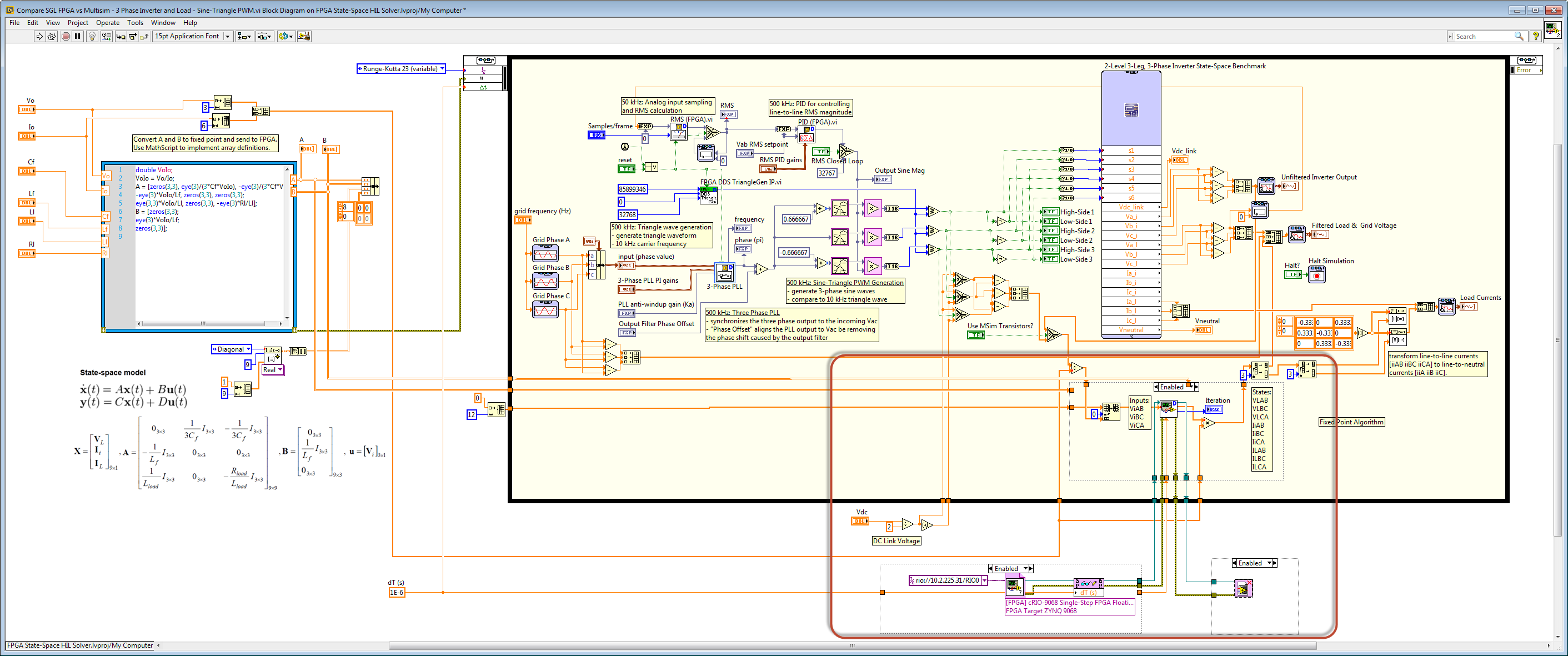
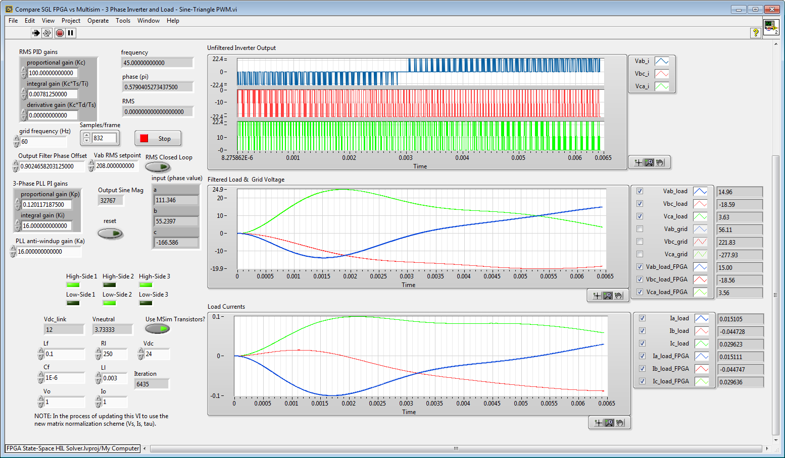
Compile the single step FPGA application and use the FPGA Interface Palette to execute the single-step application in sync with the gold standard simulation. Note that the same voltages are applied to the FPGA state-space model of the circuit and the NI Multisim model of the circuit, and they are both simulated with 1 microsecond timesteps.
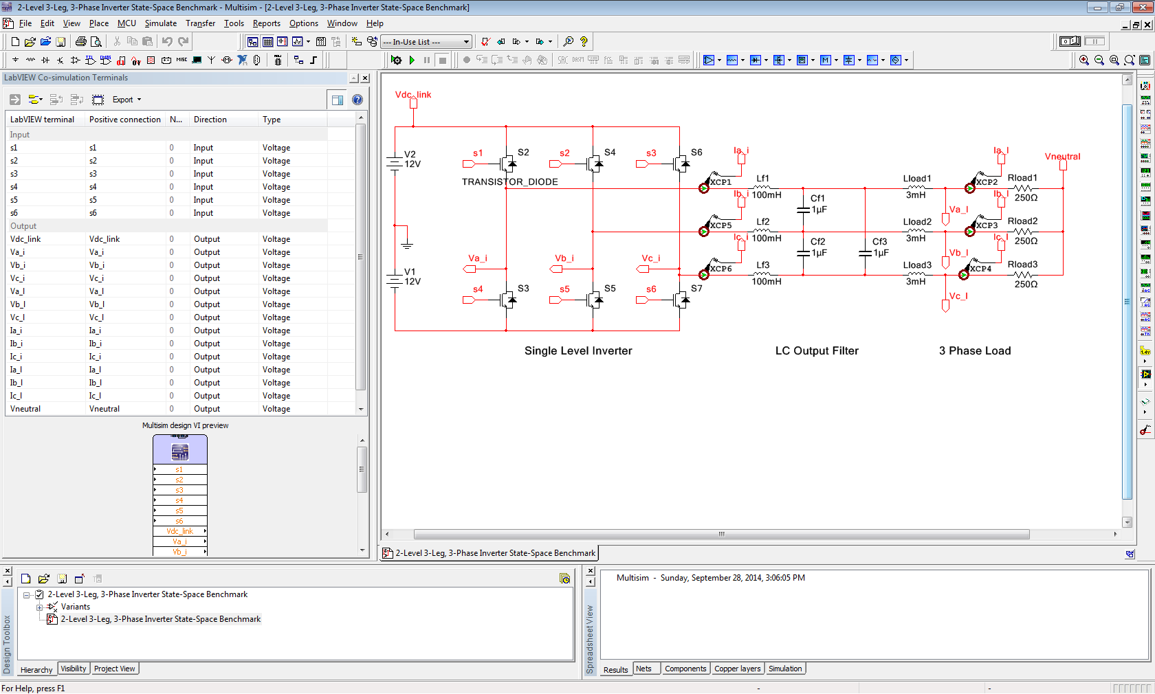
The Multisim model for the 2-level three phase power converter with line reactor filter and inductive load is shown below. Note that the Multisim Co-Simulation Interface is used to provide the point-by-point co-simulation with the Multisim circuit model. This interface is capable of time-adaptive (variable timestep) synchronized co-simulation that can provide extremely accurate simulation of the coupled dynamic interaction between heterogeneous FPGA control applications and physical circuits.
The results from the trusted algorithm (Multisim) and the FPGA algorithm under test (LabVIEW FPGA) are plotted on the same graph and the error between the two values is also displayed. In this case, the results from the FPGA state-space simulator are a good match to the Multisim results, as shown below.
Moving Real-Time Simulation to the Beginning of Development (Inverted Design V Process?)
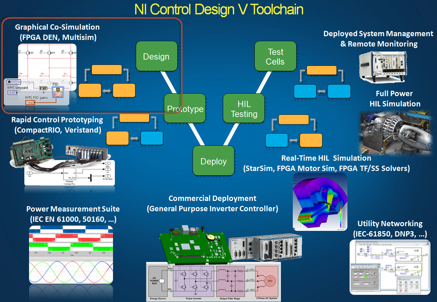
The single-step technique described above can also be utilized for hardware accelerated desktop co-simulation to facilitate the rapid development and testing of control algorithms. In this case, the LabVIEW FPGA Desktop Execution Node (DEN) is used to interface to the simulated FPGA control algorithm while the step-by-step interface to the floating point FPGA simulation model is used to simulate the physical system. In this way, graphical floating point real-time simulation in FPGA hardware can be utilized in the very first stage of the embedded system design V process shown below. This might be considered an “inverted design V process” since traditionally real-time simulation was reserved for the later stages of development. The availability of cost effective industrial embedded systems capable of executing graphical floating point math algorithms at real-time speeds, rather than expensive special purpose Hardware-In-the-Loop (HIL) test equipment, opens a wide range of possibilities that could significantly accelerate time to market for advanced embedded control systems.
Observer Based and Predictive Control
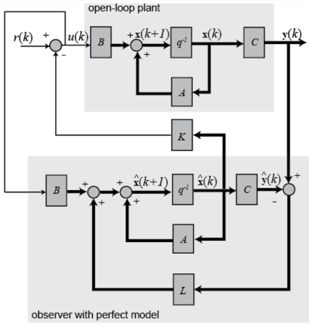
Rather than requiring an expensive, special purpose real-time simulation system, the ability to execute graphical floating point math on cost effective heterogeneous FPGA hardware and pre-validated embedded systems suitable for commercial mass deployment, opens many opportunities for innovation in embedded control design. One area of opportunity is the usage real-time simulations in the embedded control system itself for observer based and predictive control. The block diagram for a typical state-space observer based control technique is shown below.
Real-Time Simulation on Any NI LabVIEW RIO Deployment Target
The deployment curve graphic below represents the wide range of available embedded systems deployment targets available with a wide range of performance characteristics, mechanical form factors and industrial certifications and ratings as needed to meet the needs of most industrial-embedded deployment applications.
All NI LabVIEW RIO Deployment targets are capable of executing graphical floating point math algorithms for advanced control and simulation applications. Furthermore, the embedded software can be migrated with ease from one deployment target to another to provide adaptability to changing application requirements. Each point on the deployment curve is kept up to date by NI with the latest in Moore’s Law performance-per-dollar, and the migration process to port code from older to newer targets is seamless. Finally, NI provides guarantees of long term availability for most NI LabVIEW RIO deployment targets, protecting your business from the cost of expensive forced redesigns due to end of life parts—which is a formidable risk for traditional full custom embedded design of embedded computing systems.

Related Resources
· NI Power Electronics Control Design V Training Course
· Whitepaper: New ultra-fast, FPGA-based, floating-point tools for real-time power system simulation a...
· NI Power Electronics Developer Community
Feedback, Suggestions and Feature Requests
Your feedback, suggestions, questions and comments are invited.
Brian MacCleery
National Instruments
Principal Product Manager for Clean Energy Technology
09-30-2014 04:58 AM
- Mark as New
- Bookmark
- Subscribe
- Mute
- Subscribe to RSS Feed
- Permalink
- Report to a Moderator
Pretty cool. Is the version of the floating point toolkit linked to in this post very different from the IP Cores included in the corresponding Floating Point folder with the GPIC Reference Design?
It would be awesome to have this toolkit available as a VI Package.
Great stuff!
09-30-2014 09:16 AM
- Mark as New
- Bookmark
- Subscribe
- Mute
- Subscribe to RSS Feed
- Permalink
- Report to a Moderator
Good question. The GPIC Reference Design Code is now posted with the same updated version of the IP Cores library, including the new graphical floating point toolkit cores (..\IP Cores\IP Cores - LabVIEW FPGA\Floating Point).
Here is the expected directory structure assuming you unzip both the GPIC Reference Design Code and the Heterogeneous FPGA Graphical Floating Point Toolkit code in folder "C:\PowerDev\":
C:\PowerDev\IP Cores\..
C:\PowerDev\HIL Simulation\..
C:\PowerDev\GPIC\..
As a reminder, always be sure to unzip to a short directory path. Do not unzip onto your desktop.
Good feedback on using VI Package Manager. We will look into that.
Don't hesitate to let us know your feedback and feature requests on the graphical floating point toolkit.
03-02-2016 03:26 AM
- Mark as New
- Bookmark
- Subscribe
- Mute
- Subscribe to RSS Feed
- Permalink
- Report to a Moderator
VI package would be really appreciated! It is very difficult to manage the floating-point toolkit when different PCs have to be used...
03-02-2016 08:12 AM
- Mark as New
- Bookmark
- Subscribe
- Mute
- Subscribe to RSS Feed
- Permalink
- Report to a Moderator
Agreed. We are looking into VI Package Manager rather than ZIP file for future distribution. However, I can't promise we will have that in the near future. The ZIP file approach is simple and works very well as long as you unzip in a short directory path such as "C:\LabVIEW 2015" using a tool such as 7-Zip or WinZip and not the default Windows Zip utility. The paths generated by Xilinx CoreGen for IP such as the single cycle timed loop (SCTL) floating point math blocks (such as SCTL0P0, SCTL0P1 and SCTL1) are very long, and will break the code if you use a directory with even a modestly long path length. Do not attempt to put the IP core library into your LabVIEW user.lib or vi.lib folders.
Also, be sure to maintain the relative path structures for development and things will work very well.
IP cores go in a subfolder here: C:\LabVIEW 2015\IP Cores\IP Cores - LabVIEW FPGA\..
GPIC control applications go in a subfolder here: C:\LabVIEW 2015\GPIC\..
Go here to download the latest IP core library.
Guide to Power Electronics Control Application Examples and IP Cores for NI GPIC
Actually, the very latest version of the floating point IP cores is a developmental project with Proportional Resonant (PR) Control, Harmonic Compensation, and a Harmonic Waveform Extractor/Level D.... Actually, I'm planning to implement the transfer function for resonant controller with phase compensation ability from your paper Multiple resonant controller with load-adaptive phase compensation capabilities since it's clear that removing the phase shift caused by the line reactor filter (and ADC/control code delays) is required for effective harmonic compensation. This project also includes IP Builder cores for transforms like ABC/DQ and updates to the multichannel integrators (backward Euler RK1, trapezoidal) , including an IP Builder version, etc. Once development is a bit more mature, these updates will be added back into the main IP core and examples library.
03-02-2016 08:33 AM
- Mark as New
- Bookmark
- Subscribe
- Mute
- Subscribe to RSS Feed
- Permalink
- Report to a Moderator
Hi BMac, when multiple resonant controller (MRC) is implemented, try to use tustin discretization with prewarp for each resonant controller. It would reduce the discretization error. Moreover, use the real RC form instead of the ideal one, (the one in the paper) better results when discretized.
You can reach, theoretically, the nyquist frequency drastically reducing the output voltages/currents THD even when non-linear loads have to be fed. Dead-time distortion is directly compensated by the MRC, not other needs...
Cheers,
AL3
03-02-2016 08:52 AM
- Mark as New
- Bookmark
- Subscribe
- Mute
- Subscribe to RSS Feed
- Permalink
- Report to a Moderator
Sounds good. Perhaps you could share psuedocode for the discrete implementation that you recommend for the transfer function? In particular, for the Non-Ideal Resonant Controller with Phase Compensation Capability (equation 6 here).
Here's a primitive discrete implementation of the basic non-ideal resonant controller without phase compensation. My guess is that the performance would certainly be improved by spending a bit of effort on improved discretization.
Transfer Function:
Y(s) 2*wc*s
---- = ---------------------------------
X(s) s^2+2*wc*s+(n*wo)^2
Inverse Laplace:
y''(t) + 2*wc*y'(t) + (n*wo)^2*y(t) = 2*wc*x'(t)
Arrange with highest order derivative on left:
y''(t) = 2*wc*(x'(t) - y'(t)) - (n*wo)^2*y(t)
y'(t) = integral( y''(t), dt)
y(t) = integral( y'(t), dt)
Discretize:
x'(t) = dx/dt -> ( x

03-02-2016 09:04 AM
- Mark as New
- Bookmark
- Subscribe
- Mute
- Subscribe to RSS Feed
- Permalink
- Report to a Moderator
Hi BMac, I am from the DSP world even if I use LabVIEW since 1994. ![]()
My code is in C expressed as a classical difference equation: nothing new or difficult.
Unfortunately. it is not yet coded in LabVIEW FPGA....it would take some time now
Better paper is the one on journal:
For phase A, It is something like:
| err_van_f1_0 = (datas->van_ref - datas->van); | |
| out_van_f1_0 = (K_ERR_F1_0)*err_van_f1_0 +(K_ERR_F1_1)*err_van_f1_1 +(K_ERR_F1_2)*err_van_f1_2 - (K_OUT_F1_1)*out_van_f1_1 - (K_OUT_F1_2)*out_van_f1_2; |
| if(out_van_f1_0 > DUTY_MAX) out_van_f1_0 = DUTY_MAX; | ||
| if(out_van_f1_0 < -DUTY_MAX) out_van_f1_0 = -DUTY_MAX; | ||
| err_van_f1_2 = err_van_f1_1; | err_van_f1_1 = err_van_f1_0; | |
| out_van_f1_2 = out_van_f1_1; | out_van_f1_1 = out_van_f1_0; |
0: current time step, z
1: prev. time step, z-1
2: prev. time step, z-2
K_..... coeff. from discretization
If you want to change the phase compensation continuously, on-line discretization should be performed. RT target can be accomplish that.
Cheers,
AL3
03-02-2016 09:30 AM
- Mark as New
- Bookmark
- Subscribe
- Mute
- Subscribe to RSS Feed
- Permalink
- Report to a Moderator
If you have the C code for the classical difference equation, then it's easy to create the LabVIEW FPGA version in floating point. Please share that if it is available and no trouble. I typically write out the C code or "C psuedocode" for the difference equations first, and then create the LabVIEW FPGA version of the same math using floating point.
In my experience, there are often important details in the discretization that must be followed to reproduce the result. In my opinion, we should share the actual difference equations used in papers rather than only transfer functions, since different discretization methods can produce very different results. It is desirable to be able to easily reproduce the author's results, and then iterate/improve as a research community.
For example, in this paper on an inverted notch filter has a special discretization that results in better numerical performance than a simple textbook difference equation version of the z-domain transfer function of equation 1. Here is the float toolkit version. Their difference equations are different that what I got in my notebook from the original transfer function. The performance is excellent.
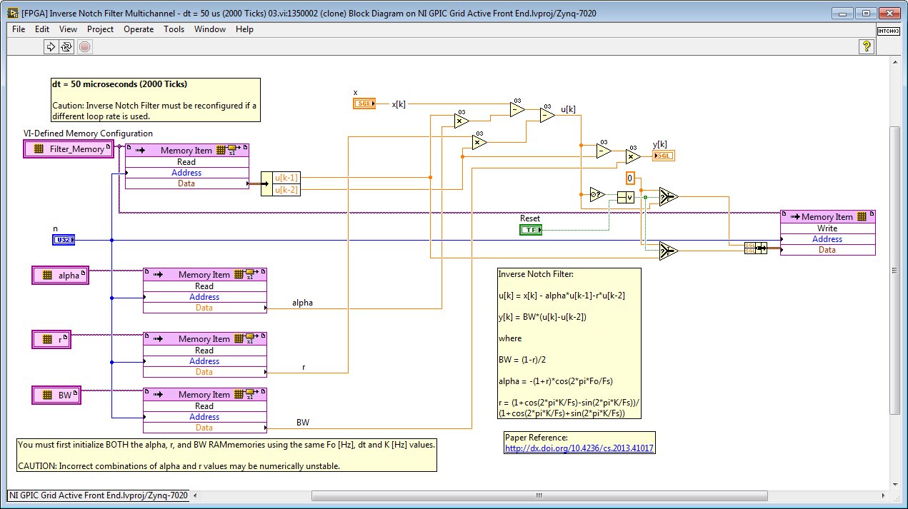
Inverse Notch Filter:
u
y
where
BW = (1-r)/2
alpha = -(1+r)*cos(2*pi*Fo/Fs)
r = (1+cos(2*pi*K/Fs)-sin(2*pi*K/Fs))/
(1+cos(2*pi*K/Fs)+sin(2*pi*K/Fs))
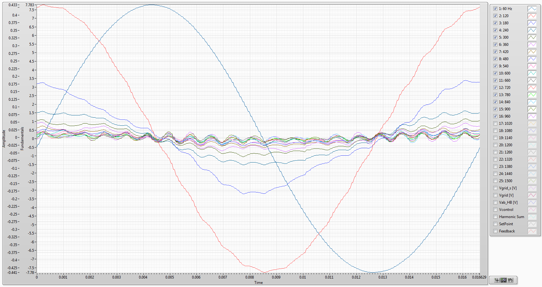
Extracted harmonic waveforms from a single-phase full bridge inverter with LR load. BTW, the inverse notch filter settings may still need some tuning but it is an interesting initial result.
03-02-2016 04:25 PM
- Mark as New
- Bookmark
- Subscribe
- Mute
- Subscribe to RSS Feed
- Permalink
- Report to a Moderator
Nice! Thank you AL3! Both papers are excellent. I'm now reading Resonant Controllers With Three Degrees of Freedom for AC Power Electronic Converters.
Now that you are using LabVIEW FPGA, do you ever want to go back to the DSP world?
