- Subscribe to RSS Feed
- Mark Topic as New
- Mark Topic as Read
- Float this Topic for Current User
- Bookmark
- Subscribe
- Mute
- Printer Friendly Page
cRIO program for controlling 9-level MMC
06-07-2015 06:37 PM
- Mark as New
- Bookmark
- Subscribe
- Mute
- Subscribe to RSS Feed
- Permalink
- Report to a Moderator
Can any one help me with a sample program or demo of a FPGA based control program which controls MMC (modular multilevel converters)
I face some problems such as making a triangular wave generator with variable phase shift
06-20-2015 12:38 PM
- Mark as New
- Bookmark
- Subscribe
- Mute
- Subscribe to RSS Feed
- Permalink
- Report to a Moderator
Hi. Sorry for the slow reply. Things are hectic!
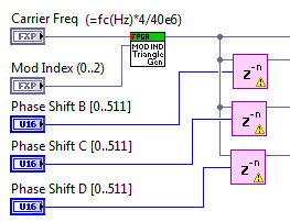
For the interleaved PWM generation with variable phase shift, the most common approach is to use the Discrete Delay IP core in LabVIEW FPGA to phase shift the triangle waveforms with configurable time delay.

The screenshot above is a modification of the GPIC Reference Design Code (unzip to short path, not desktop due to long file paths in the IP cores built using Xilinx Coregen).
Result:

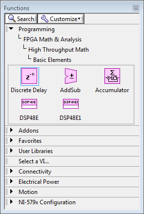
You can find the Discrete Delay block on the palette under FPGA Math & Analysis>High Throughput Math>Basic Elements.

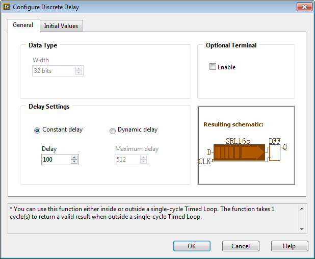
If your triangle generator and the Discrete Delay block is inside a Timed Loop running at 40 MHz, then a delay value of 1 would result in a phase shift of 25 nanoseconds. Since the maximum delay using the Discrete Delay block is 511, the maximum phase shift you can achieve using a single Discrete Delay block is 12.775 microseconds. For additional delay, you could connect a second Discrete Delay block in series, or simply run the triangle generation with Discrete delay in a separate loop running at a lower loop rate. For example, if your triangle generator with delays is running at 2 MHz, then a discrete delay value of 1 would result in a phase shift of 0.5 microseconds and the maximum delay per block would be 255.5 microseconds.
Note that if you don't need run-time variable delay, it's more efficient (in terms of FPGA resources) to hard code the delay in the configuration of the Discrete Delay node.

You may also be interested in reviewing the following presentations and papers on modular multilevel inverters based on LabVIEW FPGA and NI LabVIEW RIO hardware targets:
Dr. J. Curtiss Fox, Duke Energy eGRID Center, Introduction to the 15 MVA Grid Simulator: Challenges in Fault Ride Through Testing
Thomas Keister, TECO Westinghouse Motor Company, Power Electronics Building Blocks: Clemson Power Amplifier Units
Samuel, P.; Chandrashekhar, N.; Gupta, R., "Wind energy conversion based on seven-level cascaded H-bridge inverter using LabVIEW FPGA," Power, Control and Embedded Systems (ICPCES), 2010 International Conference on , vol., no., pp.1,6, Nov. 29 2010-Dec. 1 2010 doi: 10.1109/ICPCES.2010.5698653
Gautam, S.; Kundu, S.; Basu, P.; Gupta, R., "FPGA implementation of generalized modulation for hybrid multilevel inverter with fixed ratio DC lin...," Power Electronics, Drives and Energy Systems (PEDES), 2012 IEEE International Conference on , vol., no., pp.1,5, 16-19 Dec. 2012 doi: 10.1109/PEDES.2012.6484283
Gautam, S.; Yadav, A.K.; Gupta, R., "AC/DC/AC converter based on parallel AC/DC and cascaded multilevel DC/AC converter," Engineering and Systems (SCES), 2012 Students Conference on , vol., no., pp.1,6, 16-18 March 2012 doi: 10.1109/SCES.2012.6199078
You might want to ask the IEEE paper authors above if they would be interested in sharing their LabVIEW FPGA code on this developer community.
06-20-2015 08:14 PM
- Mark as New
- Bookmark
- Subscribe
- Mute
- Subscribe to RSS Feed
- Permalink
- Report to a Moderator
Thank you very much for your help. I am now facing a fundamental problem, I am using cRIO 9024 complete with modules 9401 and 9263. I want to generate PWM signals for the purpose of firing IGBTS, I want a triangular wave with freq higher than 5kHZ to be shown on the analog outpot of the 9263. Furthermore I want to generate the PWM signals with freq higher than 5kHZ on digital output but this does not happens. Also I am using the dead time delay made in the power electronics design kit and the minimum delay generated is 100 usec which is too high as I need only 1 usec. I feel that the cRIO is running on a low speed
Can u help me on this?
06-21-2015 12:55 PM
- Mark as New
- Bookmark
- Subscribe
- Mute
- Subscribe to RSS Feed
- Permalink
- Report to a Moderator
No problem. We should be able to sort that out very easily but it's hard to know what's going on without a screenshot or attachment of your code. Could you share that? For screenshots, first save them and then attach them using the camera button in this discussion thread editor. For attachments, first click "Use advanced editor" in the upper right and then use the Browse... button that appears in the lower left.
Based on what you described, it sounds like you might be trying to do all these different functions in the same loop. You'll need to do the analog output operation in a separate loop and using an I/O node that only has the channels for the analog output module. To share the triangle waveform data with that loop you can use an "FPGA Register" which is confusingly named because it actually creates an FPGA memory buffer that cannot be automatically accessed in LabVIEW Real-Time, or you can use a front panel control/indicator and a local data to share the data which creates a memory register that can be used to share data between loops running at different rates, and with the real-time operating system (RTOS) application.
With the C Series analog output module you are using, the maximum update rate is around 100 kHz. So, you don't want to do that in the same I/O node or the same while loop as your faster pulse width modulation (PWM) application.
Let me know if this is helpful.
06-21-2015 01:52 PM
- Mark as New
- Bookmark
- Subscribe
- Mute
- Subscribe to RSS Feed
- Permalink
- Report to a Moderator
Attached is the file I have made which should generate 2 complemantry 2 PWM signals on 2 DIO nodes and triangular wave on an analog output port. Thank you very much for your help
06-22-2015 09:04 AM
- Mark as New
- Bookmark
- Subscribe
- Mute
- Subscribe to RSS Feed
- Permalink
- Report to a Moderator
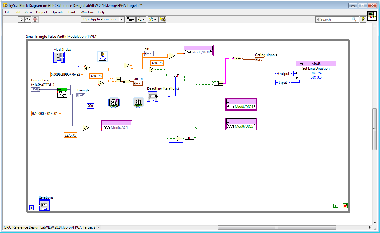
Here is a screenshot of the code you sent.

Recommendations:
1. Move the NI-9263 analog outputs to a separate while loop and pass the data to the separate loop using local variables or an FPGA register.
2. For the NI 9263 analog outputs use a single I/O node rather than two separate I/O nodes. This achieves simultaneous analog output updates and prevent arbitration over a single shared resource (the analog output node). In general, always use a single I/O node per module to prevent timing issues and resource contention issues, and only put I/O nodes that can execute at the same rate in the same while loop. The NI 9401 I/O nodes can execute at 40 MHz, whereas the analog output module can execute at 100 kHz, so you don't want them in the same loop.
3. For the NI 9401 digital outputs, use a single I/O node to avoid making separate calls into the same shared resource.
4. For scaling the signals down to the +/- 10 V range of the analog output module, use a multiply function rather than a divide function, and do the multiply operation in the separate while loop containing the I/O node for the analog outputs. A multiply operation can achieve the same effect (i.e. multiply by 1/3276.75 = 0.000305180437933928), but is much faster and uses fewer FPGA resources.
5. Note that the Iterations terminal in the while loop will eventually saturate and stop counting when it reaches its maximum value (2^32/2-1). If you need a loop iteration counter that runs forever, right-click on the loop boundary to add a shift register and increment that inside the loop.
6. Consider what data types you want to use. In this implementation you are using a mix of fixed point, integer and floating point data types in a somewhat confusing way. For example, you convert floating point to I32 before sending to the "sin-tri" chart.
7. If you are intending to scale the control sinewave amplitude in order to control the modulation index, use a version of the triangle generator that does not include the embedded modulation index to reduce resources. Please see attached versions in both fixed point and floating point.
8. The PWM carrier frequency produced by the triangle generator depends on the loop rate interval, dT [seconds]. The Carrier Frequency coefficient to use is equal to your intended carrier frequency fc(Hz) in units of Hz multiplied by 4*dT, where dT is the loop rate in seconds. Therefore, it's important to include code to measure the actual loop rate you are achieving. Here is how to do that by using the Tick Count (Ticks) output of the loop timer. Note that one tick is 25 nanoseconds if you are using the default 40 MHz base clock.

9. For maximum PWM resolution, perform the pulse width modulation inside a single-cycle timed loop (SCTL) executing at 40 MHz. This means moving any operations that cannot execute in a single clock tick outside of the loop. See the GPIC Reference Design Code (unzip to short path) for examples of sine-triangle PWM performed inside a Single-Cycle Timed Loop executing at 40 MHz.
10. The charts you are including inside the loop will only behave correctly when the FPGA is in simulation mode. Consider putting the bundle and chart functions inside a Conditional Compile structure that's configured to only execute in simulation mode (FPGA_EMULATION==TRUE). Alternately, if you use a Desktop Execution Node to test the FPGA code, the chart functions can be included in your testbench application rather than the FPGA application. See the NI Power Electronics Design V Training Course material for details.
11. The Set Line Direction operation only needs to be done once, so move it outside the PWM while loop. Put it in a sequence structure and wire something from the sequence structure to the boundary of the while loop to ensure it executes first. Or, you can set the line direction in the project configuration. Right-click on Mod 8 in the LabVIEW Project tree under the FPGA section and go to Properties.
Thanks for posting your draft code and questions. I'm sure there are other folks in this power electronics developer community with similar questions about how to program in LabVIEW FPGA to achieve the desired timing performance. Don't be shy to reply with follow up question or comments.
06-29-2015 11:43 AM
- Mark as New
- Bookmark
- Subscribe
- Mute
- Subscribe to RSS Feed
- Permalink
- Report to a Moderator
Thank you very much for your help. I have made the control. Now I am facing new challenge which is making the HIL for the MMC. I need to make a real-time model for the MMC on the cRIO using the analog output modules so I need to put the state space of the converter on the cRIO any ideas?
06-29-2015 05:34 PM
- Mark as New
- Bookmark
- Subscribe
- Mute
- Subscribe to RSS Feed
- Permalink
- Report to a Moderator
Here are a few options for real-time HIL simulation of the MMC.
1. StarSim Real-Time can run on CompactRIO or PXI Real-Time
StarSim 1.2 - A LabVIEW-based Real-Time Electrical System Simulation Software is released!
2. OpalRT eHS Solver can run on CompactRIO or PXI Real-Time. Contact OpalRT for details. See demonstration video here.
http://www.opal-rt.com/product/ehs-solver
The OpalRT power electronics teaching software for CompactRIO uses fixed circuit models, including a 3 level NPC example.
Power Electronics Teaching Software - OPAL-RT TECHNOLOGIES
3. My multi-channel floating point state-space solver which can run on CompactRIO. It includes a 3-phase 2-level inverter state-space model example.
Whitepaper: New ultra-fast, FPGA-based, floating-point tools for real-time power system simulation a...
Move Any Control Algorithm or Simulation Model to Embedded FPGA Hardware with New Floating Point Too...
After unzipping the floating point toolkit examples to a short path, you'll find the state-space solver example project here:
..\HIL Simulation\State-Space Solver\FPGA State-Space HIL Solver.lvproj
06-30-2015 03:15 AM
- Mark as New
- Bookmark
- Subscribe
- Mute
- Subscribe to RSS Feed
- Permalink
- Report to a Moderator
Dear BMac
Thank you very much. I want to ask you about option 1 which is using the StarSim, can I put the model generated from it on the cRIO? I just want to confirm this
07-01-2015 02:53 AM
- Mark as New
- Bookmark
- Subscribe
- Mute
- Subscribe to RSS Feed
- Permalink
- Report to a Moderator
Hello Mahosa,
I am Kevin from ModelingTech (the company developed StarSim). About your question, currently we have a product called StarSim Real-Time which supports customers to perform power system real-time simulation on multi-core CPU, usually the powerful PXI controllers.
And for the MMC HIL, usually it requires FPGA-based simulation solution. Our company is developing the FPGA-based power electronics simulation tool, but it is not yet ready for customers to use. But I believe that we have the capability to provide HIL system integration service for you. This video shows our DFIG RCP and HIL system.
Please contact kevin.wang@modeling-tech.com, if you are interested in ask us to develop the FPGA-based MMC simulator for you.
Best Regards,
Kevin Wang
