- Subscribe to RSS Feed
- Mark Topic as New
- Mark Topic as Read
- Float this Topic for Current User
- Bookmark
- Subscribe
- Mute
- Printer Friendly Page
USB-6001 Digital Output, Open Collector, Logic High Output Impedance
06-29-2017 11:16 PM
- Mark as New
- Bookmark
- Subscribe
- Mute
- Subscribe to RSS Feed
- Permalink
- Report to a Moderator
I'm looking on page 22 of NI's User Guide manual for the USB-6001/6002/6003 Low-Cost DAQ USB Device (manual #374259A-01, May 2014), the section titled "Source/Sink Information". According to Figure 14 "Example of Connecting an External User-Provided Resistor", when a digital I/O (DIO) pin is configured for open-collector operation, the DIO pin's output impedance for the logic HIGH state is the sum of 47 ohms + (47.5 kohms in parallel with the output impedance of the cutoff transistor). Assuming the transistor is in fact cut off, it's output impedance should be much greater than the 47.5 kohm resistance; so I'll estimate the DIO pin's output impedance as approximately 47.5 kohms.
If I select a resistance value of 5.1 kohms for the pull-up resistor, and select Vpull-up (a.k.a., VCC) to be 5 VDC, then I'd expect the voltage at the EXTERNAL LOAD node to be around 4.5 VDC, assuming a very high impedance load is connected to that node--e.g., a DMM with Zin>=10 megohms. Unfortunately, I'm not getting anywhere near 4.5 VDC; I'm seeing about 3.8 - 3.9 VDC.
I've tested multiple DIO pins (configured for open collector operation) on multiple USB-6001 devices, and they're all less than 4 VDC for a pull-up resistance of 5.1 kohm and VCC=5 VDC.
So are the manufacturing tolerances for the 47.5 kohm pull-down resistor just really, really sloppy (the calculated resistance value I'm getting is around 18.5 kohms), or is something else causing the observed low output voltage at the EXTERNAL LOAD node?
(n.b. I'm using the attached VI for testing. This VI was created w/ LabVIEW 2016.)
06-30-2017 02:39 PM
- Mark as New
- Bookmark
- Subscribe
- Mute
- Subscribe to RSS Feed
- Permalink
- Report to a Moderator
FWIW, today I did some additional testing to see if I could measure with a DMM the output impedance of a USB-6001 DIO pin configured as an output with open-collector operation. I ran my test VI (see the file attachment to my original message in this message tread) and I configured the DIO output pin for logic HIGH. This presumably turned off the transistor (see Figure 14 in the User Guide) and leaves only the 47 ohm and 47.5 kohm resistors between the DIO pin and ground. I then used a DMM to measure the resistance between the DIO pin and ground. The measured resistance value was 20.482 kohms, which correlates to my previously calculated resistance value of 18.5 kohms (see my original message). So either the User Guide is wrong, or the USB-6001s that I have were improperly manufactured, or there's something else (an undocumented "feature") that's causing this.
06-30-2017 04:22 PM
- Mark as New
- Bookmark
- Subscribe
- Mute
- Subscribe to RSS Feed
- Permalink
- Report to a Moderator
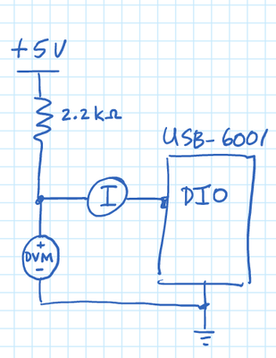
More testing. Using the test setup shown in Figure 1 I measured with a DMM the DIO pin's sink current (IDIO) and the voltage (VDIO) with respect to D GND, with the DIO pin configured as an output and open-collector mode enabled. Using Ohm's Law I then calculated the DIO pin's Thevenin resistance (RTH,DIO). The test data and calculations are shown in Table 1.
Figure 1. Test setup
Table 1. Test data and calculated RTH,DIO values
|
DIO Logic Level |
VDIO (V) |
IDIO (mA) |
RTH,DIO (Ω) |
|
LOW |
0.219 |
2.187 |
100 |
|
HIGH |
4.241 |
0.344 |
12,328 |
07-24-2017 06:08 PM
- Mark as New
- Bookmark
- Subscribe
- Mute
- Subscribe to RSS Feed
- Permalink
- Report to a Moderator
Hi jfischer, thanks for bringing this to our attention. The USB 6001 is one our low cost multi-function DAQ devices, but we will confirm whether this is expected behavior or an inaccuracy in documentation.
Angela L.
National Instruments
09-07-2018 02:42 PM
- Mark as New
- Bookmark
- Subscribe
- Mute
- Subscribe to RSS Feed
- Permalink
- Report to a Moderator
Angela
Any updates on whether this expected behavior OR an inaccuracy in documentation

